Novel graphene–oxide–semiconductor nanowire phototransistors, J. Mater. Chem. C 2014, 2, 1592-1596
Novel graphene–oxide–semiconductor nanowire phototransistors
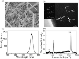
Novel graphene–oxide–semiconductor (GOS) nanowire phototransistors have been fabricated for the first time. Monolayer graphene, high-κ HfO2, and CdSe nanowire (NW) were used as transparent top-gate, gate dielectric, and conductive channel, respectively. Electric measurements of the devices reveal a clear field effect. In the dark, the on/off ratio, threshold voltage, subthreshold swing, and peak transconductance are about 4.9 × 10⁶, −1.5 V, 120 mV dec−1, and 2.3 μS, respectively. The photo-response characterization demonstrates that the gate voltage has a remarkable modulation effect on the responsivity of the phototransistors. Under 633 nm light illumination, the responsivity, gain, and specific detectivity can be as high as 1.06 × 10⁷ A W−1, 1.93 × 10⁷, and 9.68 × 10¹⁵ Jones, respectively. To the best of our knowledge, these values are among the highest reported so far for NW-based photodetectors. Our results demonstrate that GOS NW phototransistors promise a potential application in weak light detecting, which is highly desired in future optical communication or nanoscale integrated optical circuits.

http://pubs.rsc.org/en/content/articlelanding/2014/tc/c3tc32123a#!divAbstract


